Highlights
-
•
Theory and difference of SAW resonator and delay line-based sensors are reviewed.
-
•
Fabrication techniques of SAW sensors on piezoelectric and flexible substrates are presented with applications in several domains.
-
•
Study includes the challenges to fabricate flexible SAW sensors.
-
•
Future directions to overcome the fabrication challenges on flexible substrates are discussed.
Abstract
Surface acoustic waves sensors are based on piezoelectric materials. These sensors are the best choice for sensing purposes due to their unprecedented accuracy. SAW sensors are often used in biochemical sensors, drug production, chemicals agents and gas analytes as sensing devices. These systems are extremely competitive due to their compact size, high thermal efficiency, stability, and capacity to integrate wirelessly. In the past two decades, considerable research has been conducted on the manufacturing of SAW on rigid substrates. These substrates of SAW sensors preclude their use in wearable technologies. The review will cover the research conducted on flexible saw sensors to highlight limitations in this research area for future applications sensors in wearable technology. In the end, future directions and strategies have been discussed to overcome the current challenges.
Keywords
Surface acoustic waves
Flexible substrates
Flexible sensors
Wearable sensors
Piezoelectric
SAW
1. Introduction
The special electromechanical link in piezoelectric (PE) crystals gives them extraordinarily strong materials. One specific usage of piezo electric is to produce surface acoustic waves, known as SAWs, and these SAWs have amazing properties, similar to the material from which they come. In general, SAWs are mechanical waves that are confined on the elastic layer with a deterioration in the bulk of the object. In 1965, White and Voltmer's research into the development of SAWs utilizing piezoelectric substrate was a technological advance that provided a new direction to tools based on SAW [1]. Thereafter, components used in most electronic systems have been used extensively [2,3].
SAW tools are used in a broad variety of products, including wireless radio transmission as filters, spectrum duplexers, and radio frequency identification tags (RFIDs), biological sensors, medical research, biomedical, engineering, and biological sciences as microsensors for the measurement of physical parameters and biochemical detection [4,5] and as micro-actuators for microfluidic devices [6,7] and application for lab-on-a-chip [7,8].
Typically, SAW sensors are designed on conventional surfaces such as silicon (Si) or sapphire piezoelectric (PE) substances coated with PE materials like zinc oxide (ZnO) or aluminum nitride (AlN). Interdigitated electrodes (IDE) are often constructed with gold (Au) and aluminum (Al). Because of the rigid piezoelectric surfaces and metallic electrodes, these rigid SAW substrates are not applicable in the field of stretchable and transparent electronics [9]. As a result, their implementations in modular and translucent electronics are constrained [10]. Stretchable electronics have various benefits over traditional solid-state electronics due to their flexibility. Transparent electronics are an innovative technology of significant application opportunities and creativity. Numerous new flexible devices and microelectronics, such as power conditioning displays [11], electronic skin [12], and others, have been published recently. It would be enormously beneficial if SAW systems could be built inexpensively on a lightweight and flexible substrate, such as plastics that are either removable or recycled materials [13]. The development of flexile substrates and advanced functional materials has made it possible to combine SAW sensors with flexible technology and new applications of flexible saw sensors in wearable technology has become the recent topic of research.
The main aim of writing the current review is to discuss the flexible substrates and fabrication challenges of SAW sensors on flexible substrates Recent review papers on SAW sensors have emphasized the use of sensing layers, nanomaterials, and the application of these SAW sensors in a variety of areas but have paid less attention to the manufacturing difficulties associated with flexible substrates. Hence, in the following sections we have discussed the SAW sensors, sensing on flexible substrates with their application and challenges and need of additive manufacturing techniques.
1.1. Background of SAW technology
Lord Rayleigh was the first one to defined the surface acoustic wave (SAW), This is the way through which an acoustic wave is transmitted via a piezoelectric material [14]. White and Voltmer discovered another technique for generating SAW employing inter-digital transducers (IDT). From that time, such methods have been employed in a variety of regions of their various focal points [1]. A sound wave that propagates parallel to a substance's surface is referred to as a SAW. IDT electrodes constructed from metal, placed in periodic pattern on a piezoelectric material, are used to create it. A phenomenon occurs beneath the IDTs when an input sine waves with a period equal to that of the IDTs is applied, creating a SAW vertical to the direction of IDT. The SAW transmits in directions away from the IDTs on the piezoelectric material sample. The wave depth is positioned on the surface and reaches the bulk region just one wavelength deep. As a result, the energy density of the SAW is quite high. Due to this reason perhaps the sound intensity of the PE materials is 10−5 times slower than the EM wave, hence, λ is likewise a factor of 10−5 shorter, resulting in a compacted system.
An interdigital transducer (IDT) is a way of transforming electrical power into mechanical power and back again by the use of two interconnected ribbon shape metallic layers on a PE substrate. This sort of transducer is the center for the creation of a broad range of SAW devices, including delay lines, bandpass filter, resonator, and sensor [15]. SAW sensors are compact, rugged, very sensitive, reliable, and inexpensive, with a rapid real-time response. Such devices provide superior, accurate, and personalized advantages, laying the foundations for a different class of “Smart Sensors" [16].
2. SAW as sensing device
SAW instruments are the best choice for sensing purposes due to their unprecedented accuracy. The mechanism of evaluation is focused largely on the flow velocity of the sound wave conveyed further through PE substance, which is subsequently quantified by speed variation or long delay. As illustrated in Fig. 1, SAW sensors can detect a wide variety of physical parameters, including surface mass, stress, strain, torque, temperature, and pressure.
 Fig. 1
A few centimeters to several meters may be explored along SAW and delay lines, depending on the interrogation technique, voltage, and antennas. Industrial uses exist for SAW sensors, which may also be implanted into biological things. Numerous obstacles must be addressed before high temperature sensors may be used. SAW can lay claim to a considerable number of applications. By carefully choosing the metallization, it is feasible to increase fabrication accuracy and yield of resonator structures [17]. According to their construction, SAW devices are divided into two categories. Both structures are discussed in detail below [18].
The fields of applications of SAW devices are vast, comprising detectors, and referencing systems that depend on the sensitivity or resilience of particular crystal sections of different substrate materials to temperature, mechanical stress, and strain. The SAW sensor is immediately influenced by the application-specific measurement, and the sensor's sensitivity to this physical quantity is utilized. The coefficient of temperature has a considerable effect on reference and sensing devices (TK) [19].
2.1. Sensing principle of SAW sensors
The substrate, IDT, and sensing material deposited on the piezoelectric substrate all generate major effects on the properties of wave. The wave speed is a critical characteristic in the use of SAW sensing. Different piezoelectric materials have varying wave speeds. The speed of sound and temperature coefficient of frequency (TCf) of commonly used materials for acoustic devices are mentioned in Table 1 [2].
| Material |
Y–Z LiNbO3 |
128°Y–X LiNbO3 |
64°Y–X LiNbO3 |
X–112°Y LiTaO3 |
ST–X Quartz |
|---|---|---|---|---|---|
| TCf (ppm/°C) | 94 | 75 | 80 | 18 | 0 |
|
sound speed *103(m/s) |
3.488 | 3.979 | 4.742 | 3.300 | 3.159 |
Due to the SAW's rapid wave speed, it can transfer from one IDT to another in less time. This feature is largely exploited by a SAW delay line structure to determine the concentration of various analytes. Another commonly stated characteristic is the wavelength of the SAW. The SAW can only be stimulated when the transmitted signal wavelength is equivalent to the central wavelength of the SAW, that is equal to the IDT pitch. According to equation (1), relationship between the speed, wavelength, and the wave frequency is:1
On the piezoelectric substrate across which the SAW travels, a thin layer deposited is often one of the external elements affecting the SAW's wave speed. The electric field is somewhat changed when analytes come into touch with this thin layer, or a mass loading effect occurs. As a consequence, detecting gases, chemicals, and biomolecules is accomplished by detecting via measuring mass or conductivity changes of the sensor layer associated with the absorption of certain molecules [21]. Mass shifts, like the majority of other variables affecting wave speed, are difficult to quantify at the macroscopic level. This sort of change is often quantified by constructing a resonator and then monitoring the resonance frequency change. SAW resonators may be ideal for mass sensing applications due to their very high frequency. Equation (2) illustrates the link between frequency shift and fundamental resonance frequency for a common SAW device.2
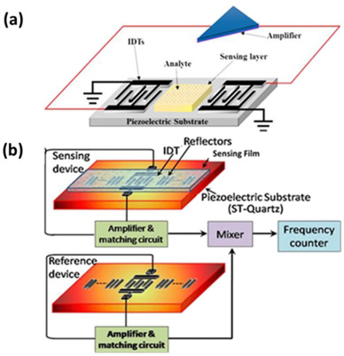
SAW sensors are built as oscillators to achieve increased sensitivity, with the SAW device acting as the frequency determining factor [24]. SAW sensors constructed to operate at substantially higher resonance frequencies, ranging from hundreds of 30 MHz–300 MHz [50], which is substantially greater than quartz crystal microbalance (QCM). This property makes SAW devices very advantageous as sensor, particularly when dealing with trace analyte concentrations [25,32]. A schematic of SAW chemical sensor-based resonator is presented in Fig. 2.
 Fig. 2
3. Flexible SAW sensors and technology
3.1. Flexible substrates for SAW sensors
The flexible technology gained more attention in early 21st century. People started to explore this technology after the publication of first US patent on flexible batteries [27]. Since then, flexible technology has made significant progress.
The small size and compatibility of sensors based on traditional substrates are highly suitable in different kind of harsh environments but the rigidity of these sensors limit their application in health care, wearable sensors and interactive robots.
Flexible sensing technology has potential to tackle these issues. The technology uses flexible properties of sensing materials which includes softness, low modulus, and ease of deformation. Polyvinyl alcohol (PVA), polyester (PET), polyimide (PI), polyethylene glycol naphthalene (PEN), paper, and textile materials are examples of common flexible materials [[28], [29], [30]]. These flexible sensors can effectively measure physiological movement, pressure change due to deformation or shape-changing things, something typical rigid sensors struggle to do. The flexible SAW sensors have also characteristics of flexible sensors and the main way to fabricate these sensors is depositing or sputtering a thin film layer of piezoelectric material on polymer substrate. Nevertheless, during this complex process to fabricate the SAW sensors, lattice mismatch has been observed between the flexible substrate and the deposited piezoelectric thin film together with difference in coefficient of thermal expansion between film and substrate Consequently, the flexible saw sensors fabrication is limited due to the availability of suitable piezo thin films and flexible substrates [31].
The most commonly used piezoelectric materials for developing thin film SAW devices on polymer substrates are ZnO and AlN. Although researchers have developed all organic SAW devices using polyvinylidene fluoride (PVDF), research on this material is still ongoing. Relatively speaking, the current mature method is to prepare ZnO/AlN piezoelectric thin films on PI/PEN. A study found that adding a multi-metal composite layer between the thin film and the substrate can improve the sensing performance of the current polymer substrate [32].
Zinc oxide (ZnO) and Aluminum nitride (AlN) are the most widely used piezoelectric materials to fabricate SAW sensors or devices on polymer substrates. Polyvinylidene fluoride (PVDF) have also been utilized for the development of SAW devices. Currently, PI/PEN are mostly used flexible substrates to develop ZnO/AlN piezoelectric thin films-based SAW flexible sensors. Also sensing performance of these existing polymer substrates can be enhanced by adding a multi-metal composite layer between the thin film and the substrate [6]. Fig. 3 shows the substrates and some commonly used materials for the development of flexible SAW devices.
 Fig. 3
3.2. Thin film based SAW devices on flexible substrate
Recently, many researchers have been working on the polymer substrates for the development of flexible SAW sensors as shown in Table 2. The properties of polymer substates during and after experiments have been summarized. The substrates like PET, PI and PEN have great advantage over traditional substrates.
| Substrate | Al foil | Flexible glass | Thin silicone | PI | PET | PEN |
|---|---|---|---|---|---|---|
| Glass transition temperature (Tg) | / | / | / | 155–360 | 70–110 | 120–155 |
| Melting temperature (Tm) | 660 | 600 | 1410 | 250–452 | 115–258 | 269 |
| Coefficient of thermal expansion (ppm C−1) | 23.21 | 32 | 5 | 8–20 | 15–33 | 20 |
| Water absorption rate (%) | / | / | / | 1.3–3 | 0.4–0.6 | 0.3–0.4 |
| Solvent resistance | fair | good | good | good | good | good |
| Transparency | poor | good | poor | poor | good | good |
| Dimensional stability | good | good | good | fair | good | good |
| Surface roughness (nm) | poor | <0.5 | <0.5 | 30 | 30 | 15 |
| Ref | [34] | [34,35] | [34,35] | [36] | [34,36] | [36,37] |
Since the first use of polymer as SAW substrate for temperature sensing in 2013, researchers have been exploring more flexible substrates for SAW sensors for the application of different physical and chemical sensors for example strain sensors, gas sensors, UV sensors, humidity sensors and temperature sensors [38].
A humidity SAW sensor developed by researchers using ZnO/PI and able to attain sensitivity of 3.5kHz/%RH [39]. Under cycle conditions, a high degree of repeatability was recorded in the humidity range of 5 %–87 % without treating surface. In another research, a woven carbon fiber was coated with PI to fabricate flexible SAW biosensor. The sensors stability was demonstrated in a continuous operation but its sensitivity under strain for biological molecules and environmental parameters was not good [40]. Hence, it is important to consider the PI parameters affecting the sensitivity.
Researchers have also explored PET as substrate to develop the SAW sensor. The ZnO based SAW strain sensor was fabricated by depositing vertically aligned ZnO thin films on PET substrate. The sensor showed good stability even after 100 cycles of bending which proved PET as good substrate under bending and deformation test [29].
The SAW sensors fabricated on polymer substrates have shown potential for various application but the challenges to develop stable and highly sensitive sensors. The main challenge is the deposition of highly crystalline and piezoelectric layer on the substrate, an important parameter to achieve good sensitivity and stability of sensor.
Also, to improve the performance of flexible saw sensors, it is crucial to explore and develop new polymer substrates. To improve device stability and sensitivity, these new materials must be more compatible with piezoelectric materials and have similar mechanical properties.
3.2.1. SAW temperature and humidity
Researchers [41] fabricated ZnO/Al based layered structures of SAW for temperature sensing by improving the TCf readings for application of temperature sensors on flexible surfaces. ZnO was deposited on an Al foil (50 ± 5 μm), a thin (200 μm), and a thick (600 μm and 1.6 mm) Al plate using DC magnetron technique. The IDEs were fabricated from 20 nm Cr and 100 nm Au, using photolithography and lift-off techniques. The wavelength λ0 of IDTs varies from 64 μm to 800 μm. They attained the highest value of TCf (−760 ppm/K) for a SAW device. The process to fabricate the device is complex.
SAW propagation properties on versatile substrates were investigated [42] by a team of researchers. Traditional deep UV photolithography and lift-off is applied to build and manufacture two port resonators. Kypton (100H,250 μm) was used as substrate. Al was considered for electrodes of 150 nm thickness. AlN film was deposited by homemade DC magnetron (Fig. 4). The thickness of AlN film is 1.23 μm and two kinds of SAW sensors were fabricated with separate wavelengths of 7.128 μm and 6 μm.
 Fig. 4
The SAW devices had been designed by photolithography with a ZnO film possessing a thickness between 1.0 μm and 4.2 μm and placed by DC sputtering on PI or PET (100 μm) or glass substrates [13]. A schematic of the flexible SAW is presented in Fig. 5 (a) and in Fig. 5 (b) the final fabricated devices is presented. A high-performance flexible SAW systems were manufactured on polymer and glass substrates, resulting in high-sensitivity temperature, humidity, UV light, and strain sensors. The unit was also used to show how versatile SAW could be used in microfluidics.
 Fig. 5
Researchers [43] fabricated AlN based Saw device for wearable temperature sensor using a thermoplastic polyethylene naphthalate (PEN) substrate. The device was fabricated by low-temperature sputtering deposition. A pattern of interdigitated electrodes was created using traditional photolithography. The clear and compact SAW delay line unit on PEN, as well as an optical micrograph of the fabricated IDT, are seen in Fig. 6(a and b).
 Fig. 6
Fig. 7 illustrates how the technology is used to create a compact temperature monitor. The AlN/PEN SAW outperformed a similar SAW technology and piezoelectric stack on silicon substrates, with a temperature coefficient frequency of ≈810 ppm°C−1.
 Fig. 7
Numerous sensors for skin temperature, biochemical perspiration sensors, and Doppler-based blood stream speed sensors can be empowered utilizing the optomechanical properties of these SAW devices on adaptable PEN [43].
Researchers also [44] developed a humidity SAW sensor using ultrathin flexible Corning Willow glass substrates (100 μm thick, and 100 mm in diameter). Sensing layer was composed of ZnO nanowires and graphene quantum dots. ZnO films were deposited by DC magnetron sputtering system. Fig. 8demonstrates the sensor fabrication, testing and packaging.
 Fig. 8
Researchers [45] fabricated two-mode flexible SAW sensor for temperature and humidity sensing. ZnO with (0002) crystal orientation was deposited on a polyimide substrate by DC sputtering. Fig. 9 shows the schematic and fabricated SAW unit for dual-mode sensor operation. It was highly vulnerable to variations in temperature. In response to cyclic changes in humidity, it showed strong repeatability. The relative humidity becomes more nonlinear as the humidity level rises. The sensitivity of SAW sensors improves as the wavelength reduces, owing to the improved properties of SAW sensors at higher frequencies. A high sensitivity of 34.7 kHz/10 % RH was obtained without any treatment of surface [45].
 Fig. 9
Jin, Hao et al. [46] produced a SAW temperature sensor by depositing ZnO nanocrystals on Kapton polyimide sheet (Toray, Dupont, thickness 100 μm), as seen in Fig. 10. A layer of ZnO was deposited on polymer surface using a direct current (DC) magnetron sputtering technique. For the SAW applications, the IDT electrodes with 20 or 50 finger pairs were deposited using 80–100 nm thick Al film. The IDT spacing was 80λ where pitch of IDT determines the λ.
 Fig. 10
Researchers also [47] designed a disposable polymer-based SAW temperature sensing system running in the GHz range using AlN and a 125 μm thick polyethylene naphthalate film, A multi-phase AlN sputter-growth process was used to make SAW AlN-based high-frequency sensors, by depositing 4.5 μm piezoelectric AlN on PEN. To acquire higher frequency sensors, a lift-off process is needed to reduce the IDT pitch. For lift-off UV photolithography on polymer-based substrates, a λ of 8 μm necessitates a finger width of 2 μm, posing a technical obstacle. Due to various low resist adhesion and the resultant irregular spin coating, as well as difficult temperature regulation, photoresist processing for a lift-off phase on a soft polymer surface is proven to be difficult. In this paper a bilayer lift-off method is applied for depositing 100 nm of aluminum and defining a polymer-based SAW unit with 2 μm long fingers. A similar SAW device manufactured on silicon substrates was compared to the flexible device. Fig. 11shows how to create a shadow region by under-etching the first layer, allowing for defect-free metal deposition, using a bilayer lift-off technique.
 Fig. 11
3.2.2. Saw strain sensors
Researchers also [9] fabricated lightweight and translucent SAW strain sensors on rigid (Corning 2318, 500 mm) and willow flexible glass structure by depositing crystalline ZnO via sputtering. IDT electrodes were fabricated from conductive ITO thin film by ultraviolet light photolithography and lift off process. Fig. 12 depicts the fabricated saw system on flexible glass.
 Fig. 12
When SAW sensors were exposed to repetitive bending test, they proved an excellent replicability and flexibility.
Another researcher [48] used a polyvinylidene difluoride substrate to fabricate a surface acoustic wave system that was used as an elemental 1-D bending curvature sensor in the network. Gold electrodes were deposited using the thermal vapor deposition process. The deposited Au electrodes had a thickness of 50 nm. The fabricated sensor is shown in Fig. 13. Finally, using a silver (Ag) conductive adhesive, lead wires were connected to four electrodes.
 Fig. 13
3.2.3. Saw sensors for respiration monitoring
A flexible SAW respiratory tracking sensor suitable for OSAS control and detection has been proposed by Jin, Hao et al. [49]. Fig. 14 depicts a diagram of the wireless passive SAW respiratory sensor device. Two types of SAW sensors, one on a versatile ZnO/PI substrate and the other on a LiNbO3 bulk substrate, were fabricated and evaluated. The piezoelectric ZnO thin films deposited on polyimide (PI) substrates were used to make the versatile SAW sensors. The interdigital transducers (IDTs) were fabricated using a typical UV light photolithograph followed by a lift-off operation, and the piezoelectric ZnO films were deposited by reactive magnetron sputtering with direct current (DC). On 128 YX LiNbO3 bulk substrates, LiNbO3-based SAW sensors were also manufactured, engineered, and fabricated for comparison [50].
 Fig. 14
Researchers [51] fabricated the flexible surface acoustic wave (SAW) sensors for ultraviolet monitoring of respiration using ZnO micro and nanostructured networks as sensing layer. The schematic of SAW sensor with ZnO 3-D tetrapodal and fabrication process of sensor is shown in Fig. 15.
 Fig. 15
The SAW devices mentioned above have some excellent properties, but they still have some drawbacks that need to be addressed appropriately. ZnO-based SAW sensors also have some difficulty when it comes to depositing thin films, which includes changes in the chemical properties of ZnO under underwater or high humidity conditions [52]. Hence, it brings challenges to the stability and reliability of ZnO as a substrate. The texture of thin films is more challenging for AlN-based thin films than for ZnO. The humidity and oxygen conditions during the deposition process have a substantial impact on the microstructure of AlN thin films [53]. ALN thin films are better for high-frequency operation than ZnO thin films due to the tremendous stress required to form a micrometer-thick layer [52]. PVDF has some disadvantages over other materials, including high manufacturing costs, complicated processing, and high prices. PVDF has strong chemical and UV resistance; however, it is also delicate and susceptible to cracking. High temperatures and humidity can alter physical qualities, potentially affecting performance. PVDF's deficiencies require immediate attention. The polymer-based SAW sensors show potential for a variety of applications, some development barriers are needed to address them. Depositing high-crystalline and piezoelectric layers on the substrate is a significant problem for achieving high device sensitivity and reliability. Developing novel organic polymer materials is vital for improving the performance of SAW sensors. To enhance long-term sustainability and sensitivity of SAW device, new materials should have mechanical properties similar to piezoelectric materials.
4. Perspective and directions for future
Research into SAW-based sensors is clearly booming, and for good reason – the potential for low-cost, reduced energy, and simplistic systems is enormous. Though SAW devices are a necessary component of electronics and microsystems, their rigid substrates and metal IDT electrodes preclude their usage in versatile and translucent electrical applications. Recent research on flexible saw devices have discussed to explore further in this field. Fabrication of flexible saw devices have been mentioned with photolithography, sputtering and lift off processes. All these techniques require expensive equipment, a clean room, high temperature and a large number of technological operations. Another essential and challenging task is the deposition of sensing layers on the flexible materials with cost effective approach. Fabrication requires additive manufacturing for the mass and cheap production of SAW sensors on flexible substrates. The additive manufacturing (AM) methods [[54], [55], [56]] have gained considerable interest prospects for rapid prototyping printed devices with a variety of features and functionality, including energy harvesting/storage, sensors, propulsion, and computing.
The flexible technology has changed over twenty years of development. The advancement can be seen from stretchable batteries to flexible sensors. The flexible SAW sensors have shown more advantages and applications in terms of sensitivity, cost and accuracy as compared to other forms of flexible sensors. Flexible SAW devices are now making remarkable progress in the selection and development of piezoelectric thin films, design and material selection of electrodes. Pressure, temperature, and strain sensors are examples of more advanced physical sensors.
Nevertheless, SAW chemical sensors have shown small progress and detection is limited to humidity. The research domain of SAW flexible gas sensors is also need more research to progress. The acoustic propagation in the flexible sensors varies when subjected to pressure or deformation unlike rigid sensors which is the main factor contributing towards the development of high-performance flexible substrates. To develop the flexible SAW sensing technology, the researchers have to overcome various technical challenges in order to produce the flexible SAW sensors like SAW gas sensors and chemical sensors.
According to the recent research, to improve the Q factor and efficiency of flexible SAW sensors, it is important to produce the high-quality materials for piezoelectric flexible thin film (such as doped AlN or ZnO) with high crystal orientation, low internal stress, a high piezoelectric coefficient, and compatibility with flexible substrates to avoid lattice mismatch. Hence, the analysis of physical properties of flexible thin films and materials for substrate is crucial for the production of high-quality SAW sensing devices. In addition, new piezoelectric thin film deposition methods should also be developed, because cutting and grinding techniques for the high-performance single crystal piezoelectric layers used in SAW devices are complex and expensive, and the utilization rate of larger materials in the manufacturing process is low, so the manufactured products not only cannot achieve complex deformation but are also prone to breakage. Furthermore, the current methods to deposit the piezoelectric thin films involve some complex and expensive techniques, hence new deposition techniques should be explored to avoid breakage of SAW devices. The flexible SAW strain sensors in bending state are still being investigated. The lack of systematic study on the strain perturbation theory of various acoustic modes, highlights the requirement of computational research. The strain-insensitive flexible substrates for SAW devices are important due to the significant impact of strain and mechanical deformation on the frequency shift of these devices. A reliable method for extracting key information from flexible SAW sensing scattering parameters and achieving anti-strain interference on surface monitoring involves combining machine learning or artificial intelligence (Al) methods.
At the production stage, in order to produce patterns on a smaller scale, higher resolution printing techniques can be implemented that enable the development of completely optimized different feature schemes. The combination of nanomaterials with additive manufacturing technology can produce low-cost sensors. Improved print resolution is also crucial for the production of high-performance electro-components. Despite rapid progress in the manufacture of functional materials for wearable intelligent equipment built on tin, other steps are necessary to address problems and impediments that may restrict further progress in the related fields [95]. As stated previously, the most exciting potential for SAW devices could be completely integrated systems that employ SAW for both procedures including production, sample handling and identification this may be the way the industry is moving towards the future. SAW applications continue to be appealing due to their versatility and compact form factor.
CRediT authorship contribution statement
Saima Qureshi: Formal analysis, Investigation, Writing – original draft. Mehwish Hanif: Conceptualization, Resources, Writing – review & editing. Varun Jeoti:Supervision, Visualization. Goran M. Stojanović: Funding acquisition, Project administration, Supervision. Muhammad T. Khan: Resources, Software, Validation.
Declaration of competing interest
The authors declare that they have no known competing financial interests or personal relationships that could have appeared to influence the work reported in this paper.
Acknowledgements
This project has received funding from the European Union's Horizon 2020research and innovation program under grant agreement No. 854194.
Data availability
No data was used for the research described in the article.
© 2024 The Authors. Published by Elsevier B.V.